
The wafer fabrication process is the most precision-critical and least tolerant of errors in semiconductor manufacturing; selecting consumables is by no means as simple as looking for “dust-free” and “anti-static” features. Wafer fabs have a set of rigorous, quantifiable, and auditable standards for evaluating nitrile gloves, focusing primarily on three key dimensions: particulate contamination control, ion residue control, and electrostatic protection stability. These three metrics directly determine wafer yield, the probability of latent failures, and the dynamic cleanliness level of the production floor; they also represent the key barriers distinguishing ordinary cleanroom gloves from those specifically designed for the semiconductor industry. Below, from the perspective of a wafer fab’s evaluation process, we break down the assessment criteria, risk pain points, and qualification requirements for each metric.
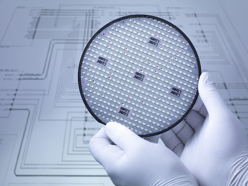
Particle Size: Monitor LPC values to control dynamic dust emission
Particles are the primary cause of wafer surface defects and microscopic foreign particle defects. Wafer fabs do not rely on “visual cleanliness”; instead, they rely solely on quantitative data from LPC (Liquid Particle Counting) measurements (particles ≥0.5 μm), which is the industry-standard, mandatory cleanliness criterion. The core logic of this assessment is that merely meeting static standards is not sufficient; true cleanliness is achieved only when no particles are shed during dynamic operations such as friction and bending. Standard nitrile gloves have a loose rubber layer and excessive surface residue. While they may pass static testing, they continuously shed microparticles when rubbed or bent, directly causing wafer defects such as white spots, pinholes, film foreign matter, and etching residues. Wafer fab access classification standards: 1. Class 10,000 / General auxiliary workstations: LPC ≤ 3,000–3,500 counts/cm² 2. Class 1,000 routine processes: LPC ≤ 1,500 counts/cm² 3. Class 100 front-end lithography/thin film/ etching processes: LPC stably ≤1,200 counts/cm² Key Evaluation Points: Prioritize gloves with a dense formulation, thorough vulcanization, and multi-stage deep cleaning with ultrapure water. This reduces floating rubber particles at the material level and removes production residues through the manufacturing process, ensuring consistently low dust emission during prolonged operations and compatibility with high-precision wafer fabrication processes.
Ionic Dimension: Monitoring Low-Level Precipitation to Prevent Hidden Corrosion Failures
Compared to visible particles, ionic residues pose the most hidden and dangerous risk in wafer fabs. Ions such as sulfur, chlorine, halogens, and metals continuously leach out and migrate during high-temperature processes and long-term storage, causing circuit corrosion, electrical leakage, parameter drift, and ghosting failures on wafers. These issues exhibit significant time lags and are difficult to trace to their source, making them highly likely to trigger customer complaints. Core Evaluation Criteria: Strict adherence to the four key purity metrics: low sulfur, low chlorine, low halogens, and completely silicone oil-free. To reduce costs, standard mass-production gloves contain large amounts of sulfur-based additives, halogen-containing stabilizers, and silicone oil release agents: the leaching of silicone oil can cause pinholes in coatings and poor lamination; sulfur, chlorine, and halogen ions can corrode precision circuits, resulting in latent wafer scrap that is completely incompatible with front-end processes. Key Evaluation Points for Wafer Fab: 1. Raw Materials: No filler additives, no silicone oil additives; strict control of migratable harmful ions; 2. Manufacturing Process: Thoroughly elute sulfides and free residues through multi-stage rinsing with ultrapure water and surface purification; 3. Testing: Provide specialized test reports for ion leaching and halogen residue for each batch; data is auditable and traceable.
Electrostatic Dimensions: Based on the body’s resistance, ensuring stable and long-lasting discharge
Bare wafers, photoresist layers, and thin-film circuits are extremely electrostatic-sensitive structures; static electricity from the human body or friction can instantly cause micrometer-scale circuit structures to break down. When evaluating ESD performance, wafer fabs do not consider the effectiveness of surface anti-static measures; they focus solely on the inherent stability of the material itself. Industry “Gold Standard” Qualification Range: Surface resistivity stable between 10⁶ and 10⁹ Ω. Key Distinction Between Genuine and Fake Anti-Static Properties: 1. Spray-Coated Anti-Static (Substandard, Obsolete Type): Anti-static liquid is merely applied to the surface layer; it rapidly degrades and the coating peels off after friction, wiping, or storage. Not only does this render the anti-static protection ineffective, but the flaking powder also causes secondary particulate contamination; 2. In-Mold Modified Anti-Static (Wafer-Specific Type): Modified through blending at the latex raw material stage, with anti-static components integrated into the material’s structure. This ensures uniform resistance, long-term stability, and no drift, peeling, or degradation even after repeated wear and friction. Wafer fab evaluation criteria: Surface spraying processes must be eliminated; ESD modification must be incorporated into the base material to ensure stable static discharge throughout the entire process, eliminating charge buildup and the risk of transient breakdown, and meeting EPA standards for static-controlled areas.
Post time: Oct-09-2026